| Technical Consulting | Training & Seminars | Scientific Investigations | EM Modeling | Test Automation | Regulatory Filing | Test Management |
|
|
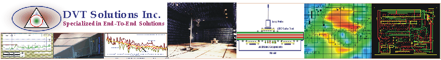
EMI/EMC/ESD TOOLS The primary source of all EMI & EMC challenges of any electronic systems is electromagnetic fields and noise currents near the PCB surface due to ASICs and radiation from cables. Knowledge of the EM fields and noise currents very near to the PCB surface, ASIC and Cables will help to identify the components, circuit and layout responsible for EMI challenge. Once the relationship is understood, Board and system designers can easily identify the root cause of the EMI challenge and can modify the board and cable design to be EMI compliant. We have created a test facility using the state of art technology and equipment for measuring the PCB, ASIC and Cable Near-Fields and currents. By using these test setups, board and system designers will find the root cause of the PCB, ASIC and cable radiations and can easily modify them to see the effect on the EMI radiation in real-time . The dedicated test setups can measure the near-fields of PCB, ASIC and cables between 10MHz – 5GHz, providing complete frequency signature of the radiation. The results are provided in two dimensional field distribution color maps at any given frequency to identify the HOT SPOTS responsible for EMI challenge. |
|
|
PRINTED CIRCUIT BOARD TOOLS
|
POWER AND SIGNAL CABLE
|